
STOCK TITAN

Qnity Electronics Inc reported $4.8B in revenue and $729.0M in net income for fiscal 2025. See the full Q financial statements: income statement, balance sheet, cash flow and ratios, each column linked to its SEC filing.

Qnity Introduces Stackplane™ CMP Slurry Platform for Advanced Packaging

(Neutral)
(Neutral)
Tags
See more from StockTitan in Google Search and AI answers. Adds StockTitan as a preferred source · opens Google
Add on Google

Supporting the transition to ‘shrink–and–stack' as part of Qnity's end-to-end advanced packaging portfolio
WILMINGTON, Del.--(BUSINESS WIRE)-- Qnity Electronics, Inc. (“Qnity”) (NYSE: Q), a premier technology solutions leader across the semiconductor value chain, has further expanded its offerings for advanced packaging with the introduction of the Stackplane™ family of slurries for chemical mechanical planarization (CMP).

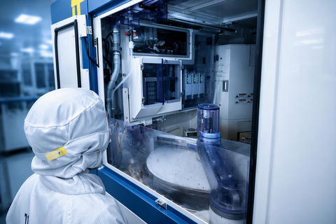
A scientist evaluates the performance of Stackplane™ CMP slurry in Qnity's polishing lab in Hsinchu, Taiwan. Qnity's Stackplane™ CMP slurries are designed for the unique CMP complexities of advanced packaging applications.

A scientist evaluates the performance of Stackplane™ CMP slurry in Qnity's polishing lab in Hsinchu, Taiwan. Qnity's Stackplane™ CMP slurries are designed for the unique CMP complexities of advanced packaging applications.

Stackplane™ slurries support the industry's move toward shrink and stack, where continued transistor scaling is paired with the stacking and integration of multiple chips to deliver the bandwidth and density that AI and high-performance computing need. Many advanced packaging programs require numerous distinct CMP steps, including planarization following hybrid bonding and through-silicon via (TSV) integration. The Stackplane™ product family brings together a comprehensive slurry portfolio to address the varied requirements of these critical CMP processes.

“Advanced packaging is creating new demands for precision, performance, and reliability across semiconductor manufacturing. As packaging technologies continue to evolve, customers need materials partners that can help address increasingly complex integration challenges,” said Kate Dei Cas, President, Semiconductor Technologies at Qnity. “Qnity already offers one of the industry’s broadest portfolios for advanced packaging, and the new Stackplane™ slurry platform further builds on that capability, supporting customers with end-to-end solutions as they advance their technology roadmaps.”

The Stackplane™ platform combines commercialized products with next-generation slurry technologies under a unified portfolio focused on advanced packaging. The platform includes slurry technologies engineered for consistent planarization at both the wafer and die level, along with the selectivity needed for advanced packaging processes. Key solutions include:

  • Stackplane™ SP1000 and SP2000 series for hybrid bonding
  • Stackplane™ SP3000 series for TSV applications
  • Stackplane™ SP4000 series for polymer CMP
  • Stackplane™ SP5000 series for emerging technologies, such as panel-level through-glass vias (TGVs) and glass CMP

Qnity will feature Stackplane™ slurries at SEMICON Taiwan, Sept. 2-4, in Taipei, Taiwan. Visitors can learn more at booth S7930 in the Materials Pavilion at TaiNEX 2 and attend a presentation by Allison Hsu, Taiwan Slurry R&D Manager at Qnity, on the TechXPOT Stage Sept. 2.

The company will also highlight the platform at the International Conference on Planarization/CMP Technology (ICPT), Oct. 19-22, in Seoul, South Korea.

Qnity experts can recommend complementary CMP pads and post-CMP cleans as part of the company's end-to-end advanced packaging portfolio. To learn more about Qnity’s comprehensive solutions for advanced packaging, visit its Advanced Packaging Innovation Hub.

About Qnity

Qnity is a premier technology provider across the semiconductor value chain, empowering AI, high performance computing, and advanced connectivity. From groundbreaking solutions for semiconductor chip manufacturing, to enabling high-speed transmission within complex electronic systems, our high-performance materials and integration expertise make tomorrow’s technologies possible. More information about the company, its businesses and solutions can be found at www.qnityelectronics.com.

Qnity™, the Qnity Node Logo, and all products, unless otherwise noted, denoted with TM or ® are trademarks, trade names or registered trademarks of affiliates of Qnity Electronics, Inc.

Media Contact
Ashley Boucher
ashley.boucher@qnityelectronics.com

Source: Qnity Electronics, Inc.

Key Terms

chemical mechanical planarization technical
Chemical mechanical planarization is a manufacturing step in semiconductor production that polishes and smooths the surface of silicon wafers so the layers built on them are even and defect-free — think of sanding and polishing a tabletop so paint goes on smoothly. For investors, it matters because this process directly affects chip yield, performance and cost: better planarization improves production efficiency and enables more advanced, profitable chips, while equipment and consumables represent significant capital and recurring expenses.
hybrid bonding technical
Hybrid bonding is a chip-assembly method that joins two silicon pieces face-to-face using very small metal and insulating connections, creating many tiny direct electrical links instead of relying on larger external wires. For investors, it matters because it lets device makers build smaller, faster and more energy-efficient processors and memory stacks, potentially improving product performance, reducing manufacturing costs, and creating competitive advantages along the semiconductor supply chain.
through-silicon via technical
A through-silicon via (TSV) is a tiny, copper-filled hole drilled vertically through a silicon chip to create an electrical connection between stacked semiconductor layers. Think of it as a short internal elevator that links floors in a skyscraper of microchips, enabling faster signal paths, smaller packages and better power efficiency. Investors care because TSVs are a key enabler of advanced chip performance, higher integration and manufacturing complexity that can affect cost, yield and product competitiveness.
through-glass vias technical
Through-glass vias are tiny, metal-lined holes drilled or etched through a glass substrate to create vertical electrical connections between different layers of an electronic package or chip assembly. They let signals, power, and heat pass through a rigid glass layer much like pipes through a wall, enabling denser, faster, and more thermally stable packaging; investors care because this manufacturing feature can affect product performance, production cost, and supply-chain complexity for companies that make advanced electronic components.
