
Toyoda Gosei Succeeds in Making Larger GaN Substrates for Next-Generation Power Devices
Toyoda Gosei Co., Ltd. and Osaka University have successfully developed a method to produce over 6-inch gallium nitride (GaN) substrates, the largest in the world.
Sentiment and the balance of points
Rhea-AI Sentiment reads the wording of the document, how positive or negative its language is on a 1 to 5 scale. The balance of points shown with the takes weighs what the document actually discloses, so the two can disagree, for example when a trial that missed its main goal is described in upbeat language.




New technology will contribute to an energy-saving society
KIYOSU,
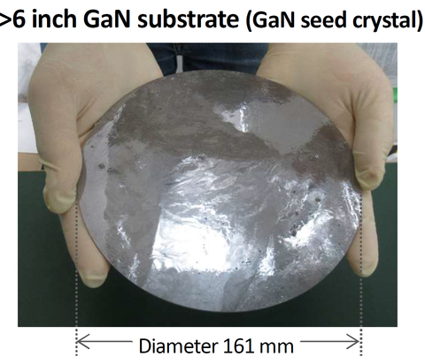
>6 inch GaN substrate (GaN seed crystal) (Graphic: Business Wire)
Power devices are widely used for power control in industrial machinery, automobiles, home electronics and more. As society moves toward carbon neutrality, the practical application and widespread use of next-generation power devices is promising as a means of reducing power loss when controlling large volumes of power in renewable energy equipment and electric vehicles. GaN power devices are one means for doing this, and higher quality and larger diameter GaN substrates are needed in the development of these devices to achieve higher productivity (cost reductions).
In a project headed by the
1
2 The technology innovation project to create future societies and lifestyles; this is a large project that includes verification of CO2 reductions from social implementation of applied products based on the development of GaN substrates.
View source version on businesswire.com: https://www.businesswire.com/news/home/20220314005004/en/
Public Relations
inquiry@mail.toyoda-gosei.co.jp
Source: