Keysight Unveils 3D Interconnect Designer for Chiplet and 3DIC Advanced Package Designs
Key Terms
chiplet technical
3dic technical
uci e technical
vtf (voltage transfer function) technical
electromagnetic-based simulation technical
Solution addresses design bottleneck by automating complex workflows

3D Interconnect Designer simplifies high-speed 3D interconnect design for silicon bridges and interposers.
As chiplet architectures are increasingly adopted, engineers face complex 3D interconnect designs for multi-die and stacked-die applications which traditional workflows struggle to handle efficiently. As a result, teams spend significant time manually optimizing the interconnects that include vias, transmission lines, solder balls, and micro-bumps while ensuring signal and power integrity in densely packed systems. This results in more design spins and longer product development cycles, creating a bottleneck that can delay product launches and increase development costs.
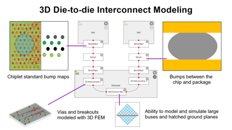
Keysight EDA software streamlines the process with a dedicated workflow for designing and optimizing 3D interconnects accurately. The tool handles complex geometries, including hatched or waffled ground planes, which are critical to overcome manufacturing and fabrication constraints, especially silicon processes such as interposers and bridges, in advanced package designs. By enabling engineers to quickly design, optimize, and validate 3D interconnects used in chiplets and 3DICs, it minimizes iterations and speeds time-to-market.
Key benefits include:
- Accelerates Design Cycles: Streamlined automation removes time-consuming manual steps in 3D interconnect design, minimizing errors and boosting first-pass success
- Reduced Compliance Risk: Validates designs against emerging standards such as UCIe and BoW, ex VTF (Voltage Transfer Function), early in the lifecycle, reducing the risk of late-stage failures that lead to costly redesigns
- Predicts Performance Accurately: Electromagnetic-based simulation provides precise electrical analysis of printed circuit boards (PCB) and package 3D interconnect designs
The solution integrates with Keysight's EDA tools as well as supporting the standalone version, enabling teams to incorporate 3D interconnect design and optimization into existing workflows. When combined with Chiplet PHY Designer, engineers can design and optimize 3D interconnects specifically for chiplets and three-dimensional integrated circuits (3DICs), ensuring accuracy and reducing costly iterations in multi-die systems.
Nilesh Kamdar, EDA Design and Verification General Manager at Keysight, said:
“With today's complexity, manual 3D interconnect design and optimization have become a significant bottleneck. By streamlining the process and providing early insights into potential issues like signal and power integrity, we're enabling engineers to get products to market faster and deliver compliant designs on tighter timelines.”
Resources
- Video: Chiplet 3D Interconnect Designer
- Webpage: Chiplet 3D Interconnect Designer
- Webpage: What’s New in High-Speed Digital Design
- Demonstration at DesignCon: The Chiplet 3D Interconnect Designer will be showcased at the Keysight booth #1039, during the conference.
About Keysight Technologies
At Keysight (NYSE: KEYS), we inspire and empower innovators to bring world-changing technologies to life. As an S&P 500 company, we’re delivering market-leading design, emulation, and test solutions to help engineers develop and deploy faster, with less risk, throughout the entire product life cycle. We’re a global innovation partner enabling customers in communications, industrial automation, aerospace and defense, automotive, semiconductor, and general electronics markets to accelerate innovation to connect and secure the world. Learn more at Keysight Newsroom and www.keysight.com.
View source version on businesswire.com: https://www.businesswire.com/news/home/20260217842809/en/
Keysight Media Contacts
Andrea Mueller
andrea.mueller@keysight.com
Fusako Dohi
+81 42 660-2162
fusako_dohi@keysight.com
Jenny Gallacher
+44 (0) 7800 737 982
jenny.gallacher@keysight.com
Source: Keysight Technologies, Inc.


