
Teradyne Introduces Titan HP Platform with Burn-In Capabilities for Advanced AI Data Center Devices
Teradyne (TER) introduced a production-ready Titan HP system with enhanced burn-in capabilities for high-power AI and other high-reliability devices.
Sentiment and the balance of points
Rhea-AI Sentiment reads the wording of the document, how positive or negative its language is on a 1 to 5 scale. The balance of points shown with the takes weighs what the document actually discloses, so the two can disagree, for example when a trial that missed its main goal is described in upbeat language.




Chipmakers can lower cost of test, factory floor space, and time to market for high-power AI, automotive, and other high-reliability devices.
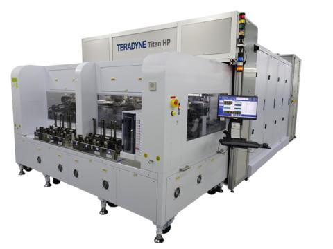
Teradyne introduces Titan HP with burn-in for advanced AI data center devices
“Our customers are being asked to ship high-power AI silicon at reliability levels that used to belong to automotive,” said Jason Zee, vice president and general manager of the Integrated Systems Test division at Teradyne. “Moving reliability stress testing onto a system level test platform means optimized reliability, which can lower cost of test, improve time to market and deliver better data on every device shipped.”
Per-site thermal control, tuned to each device's thermal and force zones, and paired with high per-device kilowatt power delivery, lets Titan HP sustain reliability-stress conditions on parts whose power draw and heat dissipation strain a conventional oven flow. The platform's asynchronous slot architecture loads and tests each slot independently, so a long stress run on one device does not idle the rest of the system, and individual sites can be serviced while the system continues to operate.
Test programs run on the Teradyne Atlas software platform, which lets engineers import existing programs or build new ones and port them to other Teradyne system level test systems. Teradyne's per-device power roadmap extends to the levels future AI accelerators are expected to require, so the same platform carries customers forward as device power grows.
Burn-in has long been standard for automotive and other high-reliability silicon. AI accelerators and cloud infrastructure devices are now entering the same category, driven by the high cost of a single failed accelerator in a deployed rack. That demand is arriving as capital, floor space, and handling capacity for dedicated oven banks come under pressure in high-volume manufacturing and OSAT facilities.
Enhanced burn-in extends Teradyne’s test portfolio, which spans the AI device supply chain from wafer to data center. As AI silicon moves through wafer probe, package test, system level test, and now reliability stress testing, Teradyne covers every device at every insertion.
Teradyne Titan HP with enhanced burn-in is available today and deployed in production. For more information, visit us at booth #1143 at SEMICON West, October 13-15, 2026, in
About Teradyne
Teradyne (NASDAQ: TER) designs, develops, and manufactures automated test equipment and advanced robotics systems. Its semiconductor and electronics test solutions span the full AI device supply chain, from wafer to data center, enabling customers to meet the quality and reliability standards the AI era demands. Its advanced robotics business deploys intelligent automation across manufacturing, logistics, and data center operations for customers worldwide. For more information, visit teradyne.com. Teradyne® is a registered trademark of Teradyne, Inc., in the U.S. and other countries.
View source version on businesswire.com: https://www.businesswire.com/news/home/20261006716626/en/
For more information
Amy McAndrews
Investor Relations
Tel 978.370.3945
investor.relations@teradyne.com
Source: Teradyne, Inc.