
Wolfspeed Expands 200 mm Silicon Carbide Portfolio with New Premium Power Substrates
Wolfspeed says it can ramp capacity at its established silicon carbide manufacturing facility as demand grows.




Premium material delivers a multi-metric leap in quality that helps silicon carbide device manufacturers achieve better yield
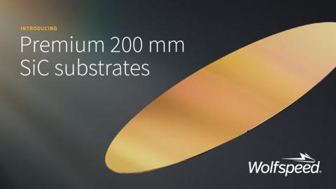
Wolfspeed expands 200 mm portfolio with premium substrate
As the SiC devices industry pushes toward higher voltages and larger die sizes, material-level quality and wafer consistency have become critical differentiators. Wolfspeed’s Premium 200 mm n-type SiC substrate delivers a multi-metric leap in quality spanning defect density, micropipe count, and wafer shape stability.
By removing variability from the starting material, Wolfspeed’s premium material gives silicon carbide device manufacturers a more predictable, higher-yielding starting material, increasing the probability of first-time design success and reducing qualification delays at a time when the margin for error is shrinking.
“Wolfspeed leads in advancing silicon carbide materials technology, and this latest addition to our 200 mm portfolio reflects our expertise behind those efforts,” said Dr. Cengiz Balkas, EVP, Materials Business Unit at Wolfspeed. “We’re giving customers a stronger foundation for developing increasingly demanding silicon carbide devices, backed by the manufacturing experience and scale to support them as needs grow.”
Wolfspeed’s Premium 200 mm n-type SiC substrate delivers fewer than 0.01 micropipes per square centimeter, or fewer than three micropipes per wafer, as validated by X-ray topography using the industry-standard method, as well as low threading screw dislocations. Combined with Wolfspeed’s proven wafer-shape and lot-to-lot consistency, the higher bare-wafer quality translates directly into better epitaxial performance achieved entirely within customers’ existing epitaxy processes.
Backed by mature manufacturing processes and deep materials expertise, Wolfspeed’s premium material delivers higher yield per lot and improved manufacturing economics. The product is orderable today, with dedicated capacity and a clear product expansion roadmap. Wolfspeed has the manufacturing confidence and ability to quickly ramp new capacity as market demand grows within the company’s established large-scale silicon carbide manufacturing facility.
Wolfspeed’s 200 mm manufacturing operations have been in continuous production since 2022, reflecting more than four years of process refinement and yield improvement and establishing a mature, reliable supply foundation for customers.
The Wolfspeed® Premium 200 mm n-type SiC substrate is available now. View products
About Wolfspeed, Inc.
Wolfspeed (NYSE: WOLF) leads the market in the worldwide adoption of silicon carbide technologies that power the world’s most disruptive innovations. As the pioneers of silicon carbide, and creators of the most advanced semiconductor technology on earth, we are committed to powering a better world for everyone. Through silicon carbide material, Power Modules, Discrete Power Devices and Power Die Products targeted for various applications, we will bring you The Power to Make It Real™. Learn more at wolfspeed.com.
Wolfspeed® is a registered trademark and The Power to Make It Real™ is a trademark of Wolfspeed, Inc.
Forward-Looking Statements
This press release contains forward-looking statements involving risks and uncertainties, both known and unknown, that may cause Wolfspeed’s actual results to differ materially from those indicated in the forward-looking statements. Forward-looking statements by their nature address matters that are, to different degrees, uncertain, such as statements about Wolfspeed’s strategic plans, priorities, growth opportunities, and ability to achieve profitability. Actual results could differ materially due to factors detailed in Wolfspeed’s filings with the U.S. Securities and Exchange Commission (“SEC”), including its most recent Annual Report on Form 10-K and subsequent SEC filings. These forward-looking statements represent Wolfspeed’s judgment as of the date of this release. Except as required under U.S. federal securities laws, Wolfspeed disclaims any intent or obligation to update any forward-looking statements after the date of this release.
View source version on businesswire.com: https://www.businesswire.com/news/home/20260927368960/en/
Media Relations:
media@wolfspeed.com
Investor Relations:
investorrelations@wolfspeed.com
Source: Wolfspeed, Inc.