
Bruker Invests in Photothermal AFM-IR to Advance Semiconductor Research
Bruker (Nasdaq: BRKR) announced accelerated development of its photothermal AFM-IR spectroscopy and installation of a Dimension IconIR system at imec on April 7, 2026.




Dimension IconIR to Support Critical Materials Characterization for Next-Generation Semiconductor Devices
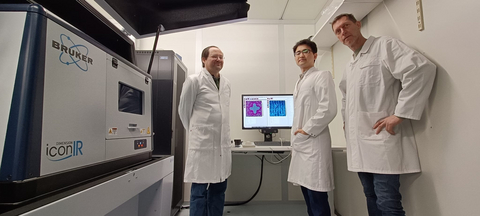
Bruker’s Dimension IconIR system at imec with (left to right) Hartmut Stadler (Bruker), Dowon Kim (imec) and Marcel Laarhoven (Bruker)
In a Joint Development Project (JDP) with imec, a world-leading research and innovation hub in advanced semiconductor technologies, Bruker has installed its Dimension IconIR system to help assess the utility of photothermal AFM-IR for addressing these critical step-function research questions. The collaboration is focused on evaluating how nanoscale chemical characterization can shed light on material behavior and interfaces that influence semiconductor process development and device performance.
“Metrology requirements for advanced semiconductor research are evolving rapidly, and together with Bruker we will assess how nanoIR technology can help address emerging requirements in nanoscale materials characterization,” said Albert Minj, senior researcher at imec and project lead of the JDP. “The IconIR system enables label-free chemical analysis with sub-5-nanometer resolution, which supports deeper understanding of EUV resist chemistry and material interactions relevant to next-generation device concepts.”
“Our collaboration with imec allows us to greatly expand the capabilities of photothermal AFM-IR in semiconductor research environments,” added David V. Rossi, President of Bruker’s Nano Surfaces and Metrology Division. “By investigating complex material systems and interfaces, nanoscale infrared spectroscopy can provide chemical insights that are impossible to access with conventional techniques.”
About Dimension IconIR
Dimension IconIR combines nanoscale infrared spectroscopy with scanning probe microscopy (SPM), delivering monolayer sensitivity, high-resolution chemical imaging, and unmatched nanoscale property mapping. Built on the widely adopted Dimension Icon AFM platform, IconIR supports samples up to 150 mm and integrates Bruker’s patented suite of photothermal AFM-IR modes. These capabilities enable precise characterization of complex semiconductor materials and structures, with hundreds of peer-reviewed publications validating its performance and correlation to FTIR techniques.
About Bruker Corporation – Leader of the Post-Genomic Era
Bruker is enabling scientists and engineers to make breakthrough post-genomic discoveries and develop new applications that improve the quality of human life. Bruker’s high-performance scientific instruments and high value analytical and diagnostic solutions enable scientists to explore life and materials at molecular, cellular, and microscopic levels. In close cooperation with our customers, Bruker is enabling innovation, improved productivity, and customer success in post-genomic life science molecular and cell biology research, in applied and biopharma applications, in microscopy and nano-analysis, as well as in industrial and cleantech research, and next-gen semiconductor metrology in support of AI. Bruker offers differentiated, high-value life science and diagnostics systems and solutions in preclinical imaging, clinical phenomics research, proteomics and multi-omics, spatial and single-cell biology, functional structural and condensate biology, as well as in clinical microbiology and molecular diagnostics. For more information, please visit www.bruker.com.
View source version on businesswire.com: https://www.businesswire.com/news/home/20260407364625/en/
Investor Contact:
Joe Kostka
Director, Investor Relations
Bruker Corporation
T: +1 (978) 313-5800
E: Investor.Relations@bruker.com
Media Contact:
Stephen Hopkins
Content Marketing Manager
Bruker Nano Surfaces and Metrology
T: +1 (520) 741-1044 x1022
E: steve.hopkins@bruker.com
Source: Bruker Corporation