
Synopsys and TSMC Partner to Accelerate AI Systems Innovation with Agentic AI and Advanced Design
Synopsys and TSMC broaden AI-driven design tools and 2nm-ready IP to help customers adopt TSMC’s most advanced nodes and packaging faster.
Rhea-AI Summary
Synopsys (SNPS) and TSMC announced expanded collaboration to accelerate next-generation AI, high-performance computing, and advanced semiconductor system design using TSMC's latest process and packaging technologies.
The companies introduced certified EDA flows for TSMC A14 across digital and analog design, including agentic AI capabilities for implementation-to-signoff convergence. Synopsys is adding AI-assisted workflows via Custom Compiler and Fusion Compiler, and new agentic AI chiplet floorplan co-optimization on the Synopsys 3DIC Compiler platform supporting TSMC 3DFabric. The partnership also advances multi-die IVR co-design on CoWoS, co-packaged optics design on TSMC COUPE technology, and an expanded 2nm-focused, silicon-proven IP portfolio spanning PCIe 7.0, HBM4, LPDDR6/5X/5, 224G Ethernet, UCIe, OTP, SLM PVT monitoring, and additional IP on N3P, N2P and compact “C” nodes from 6nm to 3nm.
Positive
- None.
Negative
- None.
Key Figures
- UCIe-A silicon demonstration
- 32G/40G
- Demonstrated on a TSMC N3P test chip integrated with a CoWoS-S interposer
- UCIe IP tape-outs
- 64G
- Completed on both 2nm and 3nm process nodes
Previous Partnership,AI Reports
-
Expanded AI-driven EDA flows, silicon-proven IP, and multiphysics signoff with TSMC
-
Expanded TSMC collaboration on certified design flows, multi-die innovation, and IP
24h Move is the share-price change in the day after each event; other market factors may also have contributed.
Key Terms
integrated voltage regulators technical
co-packaged optics technical
tape-outs technical
AI-generated analysis. How Rhea-AI works. Not financial advice.




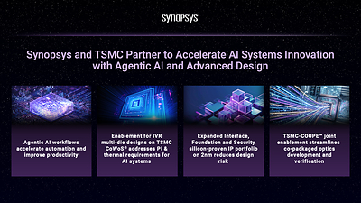
New collaborations span A14 design enablement, AI-assisted engineering workflows, CoWoS® support for multi-die designs, and unified multiphysics signoff
- Certified EDA flows on TSMC A14 accelerate design readiness for next-generation AI and HPC applications
- Collaboration on agentic AI workflows accelerates automation and improves productivity for complex analog, digital, and multi-die designs
- Continued enablement for IVR multi-die designs on TSMC CoWoS® technology addresses power integrity and thermal requirements for AI systems
- Continued joint enablement for TSMC-COUPE™ streamlines co-packaged optics development and verification
- Expanded 2nm IP portfolio and tape-out milestones including for PCIe 7.0 and HBM4 speed the development of differentiated AI, data center, edge, and automotive products
"As AI systems continue to grow in scale and complexity, customers require proven IP, intelligent design solutions, and advanced packaging methodologies that work together seamlessly," said Michael Buehler-Garcia, Senior Vice President at Synopsys. "Our joint innovations with TSMC address the continuum of silicon to systems co-design capabilities needed to accelerate development of next-generation AI and high-performance computing systems."
"Our collaboration with Open Innovation Platform® (OIP) ecosystem partners like Synopsys continues to meet the rapidly growing demands of AI and high-performance computing," said Aveek Sarkar, Director of the Ecosystem and Alliance Management Division at TSMC. "By combining certified EDA solutions and silicon-proven IP portfolio from Synopsys with our latest process and packaging innovations, we are enabling customers to push the boundaries of performance, integration, and energy efficiency to shape the future of AI."
Jumpstart Advanced-Node Adoption and Design Convergence
Synopsys and TSMC are enabling customers to transition to the latest silicon technologies with confidence. Recent achievements include A14 certification across digital, analog flows and enablement of agentic AI capabilities. These certified flows provide customers with a comprehensive methodology spanning implementation through signoff to accelerate design convergence on TSMC A14 technology.
In analog design, Synopsys is collaborating with TSMC to achieve device routing enablement on A14, a key milestone for advanced analog place-and-route automation that boosts layout productivity and speeds adoption of advanced process technologies.
Optimizing Engineering Productivity with Agentic AI Workflows
Synopsys in partnership with TSMC is leveraging agentic AI capabilities to automate analog, digital, and multi-die design workflows for greater productivity and autonomy. Synopsys Custom Compiler™ accelerates analog migration, while Fusion Compiler™ uses LLM-assisted analysis to boost productivity.
In addition, for faster heterogeneous integration in multi-die designs, a new agentic AI chiplet floorplan co-optimization flow using the Synopsys 3DIC Compiler platform automates complex floorplanning tasks and accelerates design convergence, supporting TSMC 3DFabric® technologies.
Advancing Multi-Die Design and Power Delivery with TSMC
As next-generation AI systems drive unprecedented power delivery requirements, integrated voltage regulators (IVRs) emerge as a key technology for improving power efficiency and power integrity in multi-die designs. Synopsys 3DIC Compiler platform now enables designers to efficiently co-design and simulate IVR on TSMC CoWoS® technology in a unified environment for advanced packaging.
Enabling the Future of Co-Packaged Optics
Optical interconnect technologies are becoming increasingly important for efficient, high-speed system connectivity. Synopsys continues to work with TSMC to enable co-packaged optics (CPO) design on TSMC COUPE™ technology through an integrated photonic and electronic co-design flow spanning 3DIC implementation, multiphysics analysis, and optimization. Both companies help mutual customers efficiently develop and verify advanced optical interconnect architectures for systems using multi-die designs.
Providing a Foundation of Silicon-Proven IP for Next-Generation AI Systems
Synopsys in collaboration with TSMC is accelerating next-generation AI, HPC, data center, edge, and physical AI systems with the industry's broadest portfolio of silicon-proven Interface, Foundation, and Silicon Lifecycle Management (SLM) IP optimized for TSMC's advanced process technologies. Building on first-silicon success across TSMC's N5, N3P, and N2P technologies, Synopsys continues to expand its ecosystem-ready IP portfolio to help customers reduce risk, accelerate time-to-market, and achieve aggressive power, performance, and scalability goals.
On TSMC's N2P process, Synopsys achieved key IP enablement and tape-out milestones for AI and HPC designs, including PCIe 7.0, HBM4, LPDDR6/5X/5, 224G Ethernet PHY, UCIe, OTP, and advanced SLM process, voltage, and temperature (PVT) monitoring IP. Together, these solutions deliver the high-bandwidth connectivity, memory performance, and real-time system intelligence needed for increasingly demanding AI workloads.
Advancing multi-die innovation, Synopsys demonstrated UCIe-A 32G/40G silicon on a TSMC N3P test chip integrated with a CoWoS-S interposer, validating high-speed die-to-die connectivity for AI systems. Synopsys recently completed 64G UCIe IP tape-outs on both 2nm and 3nm process nodes. The IP provides in-system visibility with embedded DFT capabilities.
Synopsys also recently expanded its portfolio of silicon-proven Foundation, MIPI, and memory IP for TSMC's N3P, N2P, and is developing IPs on compact "C" process technologies from 6nm through 3nm. These solutions enable higher integration, lower power consumption, and faster deployment of intelligent, feature-rich systems across AI, data center, networking, mobile, automotive, and edge AI applications.
Additional Resources
- Blog: Multi-Die, Multiphysics, and the New Rules of Chip Design
- eBook: Multiphysics Fusion Technology for Multi-Die Designs Explained
- eBook: Silicon Starts with Proven IP eBook | Synopsys
About Synopsys
Synopsys, Inc. (Nasdaq: SNPS) is the leader in engineering solutions from silicon to systems, enabling customers to rapidly innovate AI-powered products. We deliver industry-leading silicon design, IP, simulation and analysis solutions, and design services. We partner closely with our customers across a wide range of industries to maximize their R&D capability and productivity, powering innovation today that ignites the ingenuity of tomorrow. Learn more at www.synopsys.com.
© 2026 Synopsys, Inc. All rights reserved. Synopsys, Ansys, the Synopsys and Ansys logos, and other Synopsys trademarks are available at https://www.synopsys.com/company/legal/trademarks-brands.html. Other company or product names may be trademarks of their respective owners.
Contacts
Media
Kelli Wheeler: kelliw@synopsys.com
Pete Smith: pete.smith@synopsys.com
corp-pr@synopsys.com
 View original content to download multimedia:https://www.prnewswire.com/news-releases/synopsys-and-tsmc-partner-to-accelerate-ai-systems-innovation-with-agentic-ai-and-advanced-design-302887861.html
SOURCE Synopsys, Inc.